The M20 firmware
by Davide BucciDescription of the M20 bootstrap procedure
In this section, we try to provide a short description of the code contained in the 8kB ROM which performs the diagnostic tests at the system startup and boots the operating system. The rom contents (revision 1.21) have been dumped and disassembled by Chris Groessler and the source can be found in the file rom.s
At the startup, the Z8001 fetches its status (named FCW) at segment 0, offset 2 and the program counter (PC) at segment 0, offset 4. The ROM code begins with:
begin:  .word   0               !
        .word   0xc000          ! FCW at reset
        .long   reset           ! PC value at reset
In this operation, all interrupts must be disabled and the system must be designed in order that a NMI is not sent to the Z8001 during this initialization phase. In the M20, the memory management system is obtained by using several PROMs, which map the logical segments into the physical ones. In the boot phase, the system is configured with the 8kB boot ROM at the segment 0 and the code is executed.
At first, the screen is initialized (after determining if it is a color or black and white version). Then, tests are performed in order to verify system integrity. At each test, a shape is drawn on the screen and if the test is unsuccesful, the computer hangs up, showing the last shape drawn. In a working system, the screen has not the time to lighten up and the end user seldom sees the shapes.
The beginning of the tests appears like it follows, drawing a triangle on the screen:
    ! give some indication on the display where in the self-test we are
        ld  scrmem,#0x1000          ! 0001000000000000
        ld  scrmem + 0x40,#0x2800   ! 0010100000000000
        ld  scrmem + 0x80,#0x4400   ! 0100010000000000
        ld  scrmem + 0xc0,#0xfe00   ! 1111111000000000
scrmem points at the very beginning of the video memory. As the M20 graphic adapter is used has a 512 pixel width line (and one pixel corresponds to one bit), the address scrmem+0x40 corresponds to the beginning of the second line and so on.
Right after drawing the triangle, the program perform a series of basic test on the CPU: use of registers, addressing modes, operation like multiplication and division, complement. The screen is then cleaned and a small square is drawn. The ROM consistency is tested, with a checksum algorithm.
The next phase is started by drawing a diamond on the screen and the RAM is tested. In a similar way, 4 small vertical lines indicates that the test for CPU calls and traps is being done. This way, if a test fails, the geometrical pattern remains on the screen and tells which test has failed.
Error messages at startup
Here is a list of the possible error codes that can be shown at the startup.
| Message given: | Error condition: |
|---|---|
| Triangle | CPU problems |
| Diamond | RAM test failed |
| 4 vertical lines | Test CPU instructions call and trap failed |
| EC0 | 8255 error parallel interface |
| EC1 | 6845 error screen controller |
| EC2 | 1797 error disc drive controller |
| EC3 | 8253 error timer circuit |
| EC4 | 8251 error keyboard interface circuit |
| EC5 | 8251 error RS-232 interface |
| EC6 | 8259 error interrupt controller |
| EK0 | Keyboard not responding |
| EK1 | Keyboard responding, but autotest failed |
| ED0 | Error floppy 0 |
| ED1 | Error floppy 1 |
| ED10 | Error hard disk |
| E10 | Non vectored interrupt error |
| E11 | Vectored interrupt error |
| DISK DRIVE NOT READY | No disk in drives |
| INVALID BOOT FILE | The disk is not bootable |
| DISK ERROR XX | Error during disk access. The XX is an hexadecimal 8 bit code. Each bit means:
|
Firmware revisions

We know two main revisions of the M20 firmware: 1.x and 2.x. The main difference seems to be the ability to recognize the Alternate Processor Board (APB8086) card and the hard disk.
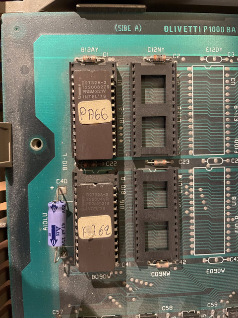
If you have the Italian "BC" (Business Computer) version with the firmware 1.0, you will probably have the EPROMs PA62 and PA66 installed. Those prevent some graphical commands to run. You can not use LABEL, for example. Having nice graphics was considered frivolous in 1981 for a business-oriented computer whose hardware was perfectly capable of displaying them? As said before, this version of the firmware does not check for the presence of the Alternate Processor Board (APB8086).
The picture on the right shows the PA66/PA62 (BIOS v. 1.0 for the Italian BC) EPROMs installed in a rev. D motherboard.
The Olivetti M20 firmware is contained in two 2732 EPROMs. The first one contains the least 8 significative bits of the 16-bit word and the second one contains the 8 most significative bits. Both EPROMs are accessed at the same time as, as we know, the Z8001 is a 16-bit processor. You can read 2732 EPROMs with the widespread TL866II+ programmer, but some of them require a program voltage higher than what the 18V that the TL866II+ can provide. You can build an adapter and provide the required voltage externally.
| File | Revision | Notes |
|---|---|---|
| Firmware_1_0.zip | 1.0 | The standard 1.0 firmware. |
| Firmware_1_0_BC.zip | 1.0 (BC) | Can not access some graphic functions of the machine. They are marked PA66 and PA62. Models sold outside Italy did not have that limitation. |
| Firmware_2_0d.zip | 2.0d | To upgrade from version 1.0, you should change the ZA jumper from ZA-2 to ZA-1, to correctly address the disk drives with the new firmware. |
| Firmware_2_0f.zip | 2.0f | To upgrade from version 1.0, you should change the ZA jumper from ZA-2 to ZA-1, to correctly address the disk drives with the new firmware. The original EPROM s from Olivetti were marked PA77 and PA78. |

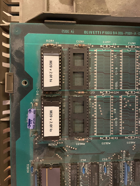
On the motherboard rev. D, the high byte EPROM should be installed on the left (keeping the Z8001 processor towards you), in the slot marked B12AY, and the low byte on the right in the slot B09DW. Be careful to align correctly the pins: the sockets are slightly larger than the 2732 EPROMs. Two rows of pins should be left empty on the top of the chip. Probably, Olivetti had in mind to install larger EPROMs such as the 2764 for future upgrades, as well as another pair of EPROMs.
The picture on the right shows two EPROMs prepared in 2024 and containing the 2.0f version of the firmware, installed in a rev. D motherboard.
The 2.0f firmware notoriously contains the "spider" easter egg. If you depress COMMAND-S while the computer is waiting for a system disk, a little spider crawling on the screen will appear!

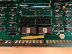
The location of the EPROMs in a rev. G board is slightly different. The picture on the right shows them. In the original Olivetti naming notation, the rev. 2.0 EPROMs were called PA77 and PA78. All of those had the little handwritten label. How cute! This picture was kindly sent by Benjamin Eberhardt.
Page log
- Nov. 3, 2024 - added mention to PA77 and PA78 EPROMs
- Oct. 22, 2024 - added Benjamin's pictures of the EPROMs in a rev. G board.
- Oct. 6, 2024 - expanded and reorganized. Added instructions about firmware upgrade.
- Jan. 10, 2016 - updated to the newer version (2012) of rom.s file.
- Oct. 7, 2006 - some improvements.
- Aug. 4, 2006 - original version of the page.
Olivetti is a registered trademark of Telecom Italia. This site is not related to Olivetti nor to Telecom Italia. The material presented is meant for personal use only and is shared in a "fair use" spirit. If you own the copyright of some of the stuff presented here and you think it should be removed, please contact the webmaster.


